High Speed PCB Layouts Design
At NextEraWave,
We deliver high-speed PCB layout solutions tailored for systems demanding low jitter, high bandwidth, and electromagnetic resilience. Our designs account for signal integrity, impedance control, and differential pair routing across DDRx, PCIe, USB, and SerDes interfaces.
Our PCB Design Capabilities
- We create precise and optimized circuit designs tailored to your requirements.
- Expertise in single-layer, multi-layer, and HDI PCB for complex applications.
- Specializing in high-frequency, signal integrity-optimized layouts for cutting-edge applications.
- Custom PCB designs for diverse applications, including wearables, aerospace, and industrial electronics.
- Optimized heat dissipation, power integrity, and reliability for long-term performance.
- Pre-manufacturing validation with SPICE simulations, SI/PI analysis, and thermal modeling.
We ensure that all our PCB designs meet global quality, safety, and environmental standards, including:
✔ IPC Standards – Compliant with IPC-2221, IPC-6012, and IPC-A-600 for PCB design, fabrication, and assembly.
✔ RoHS & REACH Compliance – Environmentally friendly designs with lead-free materials.
✔ EMI/EMC Guidelines – Ensuring minimal electromagnetic interference for optimal performance.
✔ ISO 9001 & ISO 13485 – Meeting rigorous standards for industrial and medical device applications.
We offer comprehensive PCB testing and validation to ensure reliability, durability, and performance, including:
🔍 Signal Integrity (SI) & Power Integrity (PI) Testing – Detecting noise, distortion, and voltage fluctuations.
🔍 Thermal Analysis – Evaluating heat dissipation to prevent overheating issues.
🔍 EMC/EMI Testing – Ensuring compliance with electromagnetic compatibility standards.
🔍 Prototype Debugging & Functional Testing – Identifying and resolving design flaws before production.
We provide end-to-end design and manufacturing services, ensuring a seamless transition from concept to production:
🛠️ Design for Manufacturability (DFM) – Optimized PCB layouts for efficient production and assembly.
🛠️ Design for Testability (DFT) – Ensuring easy debugging and testing during manufacturing.
🛠️ Prototype to Mass Production – Scalable solutions from low-volume prototypes to high-volume manufacturing.
🛠️ Assembly & Quality Control – Rigorous quality checks, including AOI, X-ray inspection, and functional testing.
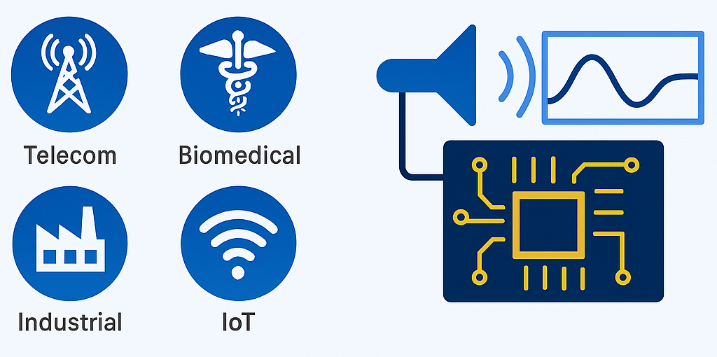
Custom Antenna Design & RF Circuit Development
Industry-Focused Consultancy
Testing & Measurement Services
Contact
- NEXTERA WAVE PRIVATE LIMITED 04 BDA Community Hall Valagerahalli Kengeri, RV Niketan Bengaluru-560059 Karnataka India
- +91 94922 35011
- info@nexterawave.com
Brochures
“Empowering innovation with quality and commitment, we deliver solutions that drive success.”